TL;DR
- This blog is designed for electronics startups, R&D engineers, product designers, hardware developers, and educational institutions seeking a clear understanding of the design-to-fabrication process and the importance of pcb prototyping in modern electronics development.
- The article explains the complete design-to-fabrication workflow,from concept development and schematic design to PCB layout, file preparation, fabrication, assembly, testing, and optimization.
- It highlights how in-house PCB prototype machines enable rapid production, reduce turnaround time, protect intellectual property, and allow faster design iterations compared to outsourced manufacturing.
- The blog emphasizes that fabrication transforms digital designs into physical boards, while thorough testing and validation ensure signal accuracy, power stability, and performance reliability before mass production.
- By leveraging subtractive and additive methods, along with rapid iteration cycles, pcb prototyping significantly accelerates time-to-market and enhances product innovation across industries like IoT, medical, automotive, and aerospace.
The modern electronics industry is highly competitive and fast-moving; success depends on speed, accuracy, and innovation. It is crucial to quickly transform an idea into a working circuit board whether you are a startup developing an IoT device, an R&D engineer testing a new circuit architecture, or a school or college educator training your future engineers. This is where PCB prototyping becomes transformative.
The design-to-fabrication cycle using PCB prototype machines enables engineers to transition from schematic design to a fully operational PCB in hours or days instead of weeks. PCB prototype machines have transformed the current development of electronics by allowing rapid development, cost reduction, and in-house manufacturing.
We will delve into the entire design-to-fabrication cycle process, the role of PCB prototyping in all these phases, and how PCB prototype machines improve speed, quality, and efficiency.
Explore More Insights:
- From Idea to Prototype: How Students Build Real Projects with PCB Prototyping and 3D Printing
- What Is a PCB Prototyping Machine? Working, Types, and Applications.
- How Technical Training Institutions Can Prepare Students for Semiconductor Careers
Understanding PCB Prototyping
PCB prototyping is the process of creating an early model of a printed circuit board to test and validate the design before full-scale manufacturing. Instead of submitting designs to third-party manufacturers and waiting weeks for fabrication, engineers can use PCB prototype machines to fabricate boards in-house.
Why PCB Prototyping Matters
- Reduces design errors before mass production
- Speeds up product development cycles
- Minimizes manufacturing risks
- Lowers long-term production costs
- Enables rapid design iterations
In competitive industries such as automotive electronics, medical devices, aerospace systems, and consumer electronics, pcb prototyping significantly shortens time-to-market.
The Role of Fabrication in PCB Prototyping
Fabrication is the stage in pcb prototyping where the digital design is transformed into a physical board. A PCB is manufactured in every prototyping cycle and tested to ensure proper functionality and reliability.
The bare board is first fabricated, containing copper traces, pads, and drilled holes but no components. Subsequently, components are mounted using through-hole soldering or surface-mount technology (SMT) or a combination of both, resulting in a complete PCB assembly (PCBA) ready for testing.
This process could take a few days or weeks depending on the complexity of the board and the capacity of the manufacturing. However, rapid and additive fabrication methods now enable faster pcb prototyping, sometimes delivering functional boards within a single day.
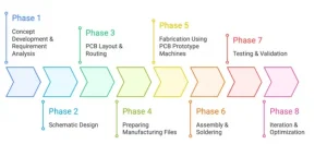
Overview of the Design-to-Fabrication Cycle
The design-to-fabrication cycle in pcb prototyping typically includes:
- Concept Development
- Schematic Design
- PCB Layout & Routing
- File Preparation
- Fabrication Using PCB Prototype Machines
- Assembly & Soldering
- Testing & Validation
- Iteration & Optimization
Each phase builds upon the previous one, forming a streamlined workflow that ensures precision and performance.
Design-to-Fabrication Cycle Using PCB Prototype Machines
The design-to-fabrication cycle using PCB prototype machines is a streamlined process that converts an electronic concept into a fully functional printed circuit board. This cycle lies at the core of modern PCB prototyping and allows engineers to rapidly proceed between design and testing without losing precision or costs. Organisations can save a lot of time in the development process and enhance product reliability with a combination of digital design tools and in-house fabrication technology.
Phase 1: Concept Development & Requirement Analysis
Any PCB project starts with a well-defined concept. During this first step, engineers determine the functional requirements, input and output specifications, the power constraints, operating conditions, and compliance standards to be used. All this defines the technical direction of the design and ensures the final product performs as intended and meets regulatory requirements.
Concurrently, feasibility studies are conducted to check on components availability, limitations of board size, cost, and overall performance requirements. Proper planning at this stage establishes a strong foundation and ensures a more efficient and streamlined PCB prototyping process in the subsequent development phases.
Phase 2: Schematic Design
The schematic is the conceptual outline of a PCB. Using Electronic Design Automation (EDA) programs like KiCad, Altium Designer, Autodesk Eagle, and OrCAD, engineers develop a detailed circuit diagram that defines the electrical connections between all components. This process converts the conceptual requirements into a formal electrical design which becomes the reference point of the whole process of building the prototype PCB.
In schematic development, special emphasis is placed on proper choice of symbols, proper net labeling, proper planning of power distribution, proper decoupling capacitor placement, and elementary signal integrity guidelines. Prior to layout, Engineers perform Electrical Rule Checks (ERC) to detect and resolve potential issues. There is a high degree of accuracy required at this point because any small schematic mistakes may cause expensive fabrication issues when pcb prototyping.
Phase 3: PCB Layout & Routing
After completing the schematic, the design is imported into PCB layout software and the physical design of the board is created. This phase includes deciding board sizes, the layer stack-up, component placement, routing, via placement, and the design of ground planes. In proper layout planning, it is necessary to keep the board compact, efficient and in line with the manufacturing requirements.
Signal integrity, thermal management, EMI/EMC control, controlled impedance, and high-speed routing practices should be taken into careful consideration by the engineers during layout. Design Rule Checks (DRC) are performed to ensure manufacturability and design standard adherence. This stage is critical in pcb prototyping because layout quality directly influences the electrical performance, reliability, and functionality of the end board.
Phase 4: Preparing Manufacturing Files
The PCB design should be exported into industry-standard manufacturing formats before fabrication begins. These typically include Gerber files for copper layers, drill files (Excellon format) for hole specifications, a Bill of Materials (BOM), and pick-and-place files for automated assembly. These files make it possible to have accuracy and efficiency in fabrication and assembly processes.
These outputs must be carefully validated to prevent machine errors during PCB prototyping. Gerber viewers are also used to check the alignment of the layers, precision of the drills and integrity of the footprint by engineers when looking at the data that is being exported. Close validation at this point helps to eliminate expensive errors and a smooth transition to fabrication.
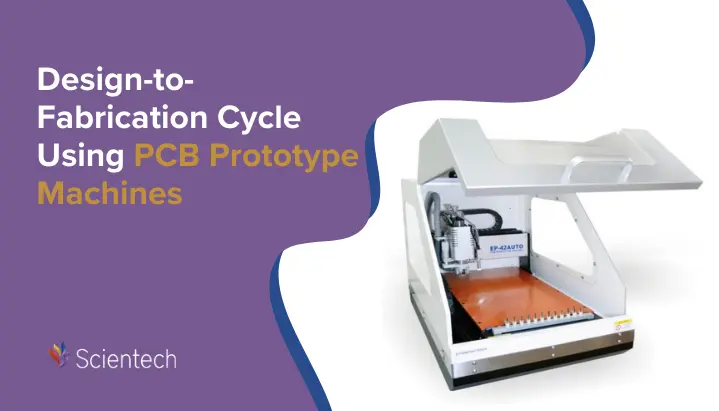
Phase 5: Fabrication Using PCB Prototype Machines
This is the point where a digital design is converted to a physical circuit board. During fabrication, the finalized design files are used to create precise copper traces and structural features on the PCB. This is one of the key processes in the pcb prototyping process because it makes the idea a reality to be tested and validated.
PCB prototype machines are small, in-house fabrication systems which allow engineers to mill, drill, and cut circuit boards out of copper-clad substrates. These machines enable rapid and controlled manufacturing, significantly reducing turnaround time and supporting faster design cycles.
Phase 6: Assembly & Soldering
The next stage in the PCB prototyping cycle involves mounting electronic components onto the fabricated board. This is made through proper assembly to make the prototype reflect the desired final product and work well when tested.
There are two main assembly techniques. Through-hole assembly involves inserting components into pre-drilled holes, creating strong mechanical bonds and it is applicable in power electronics and in other components that require a strong mechanical bond. Surface Mount Technology (SMT) is a method that mounts components on the surface of the board, which enables it to occupy a small area of the layout and a high concentration of components. The various methods of soldering are used like manual soldering, reflow soldering, and wave soldering based on the complexity of boards and production requirements. Accurate assembly at this stage ensures that testing reflects real-world performance conditions.
Phase 7: Testing & Validation
No PCB prototyping cycle is complete without testing and validation. After assembling the board, the engineers carry out a series of tests that are meant to verify that the prototype works accordingly. Common tests include visual inspection, continuity testing, functional testing, oscilloscope measurements, thermal testing, and load testing. Such processes assist in identifying flaws in manufacturing, soldering problems or flaws in designs at the initial stage of the design.
In this phase, the engineers check the accuracy of signals, power stability, noise, and other levels of performance standards. Should any problems be found, the design is revised and improved and re-prototyped. The process of doing this over and over again makes sure the final PCB is able to perform, be reliable and meet quality expectations before passing on to production.
Phase 8. Iteration & Optimization
Rapid iteration is one of the most important benefits of PCB prototype machines. The design can immediately undergo improvements thus numerous refinements can be made within a limited time. This greatly increases innovation and time-to-market.
Types of PCB Prototyping Methods
1. Subtractive Method
- Copper is removed from the board using milling tools.
- Ideal for rapid prototyping.
- Clean and chemical-free process.
2. Additive Method
- Copper is deposited only where required.
- Used in advanced pcb prototyping setups.
Fabrication Steps Using PCB Prototype Machines
- Secure the copper-clad board onto the machine bed.
- Load and verify Gerber design files.
- Generate automated tool paths through the control software.
- Mill copper traces according to the layout.
- Drill component holes and vias.
- Cut the board outline to finalize the structure.
Conclusion
The design-to-fabrication cycle using PCB prototype machines represents a significant breakthrough in the current development of electronics. Through the integration of digital design and in-house manufacturing, an engineer can develop a concept for a working circuit board within the shortest time.
PCB prototyping eliminates risk, expedites innovation and allows engineers to perfect the design with accuracy and confidence. Be it designing the latest IoT gadgets, a high-level medical apparatus, or high-performance industrial controllers, it is important to master the pcb prototyping cycle.
As industries demand faster development cycles, tighter tolerances, and higher performance standards, PCB prototype machines will remain central to accelerating innovation and reducing product development risk.