
Project-based learning forms an integral part of Engineering Courses at the undergraduate and postgraduate levels, providing opportunities to students to convert their ideas into exciting prototypes. These projects open new avenues for students to work on various real world problems and address challenges in innovative ways. This method also helps them apply theoretical knowledge to find tangible solutions by fostering better appreciation of engineering principles, acquired through textbooks.
Let’s explore how these projects, often mandated by the curriculum, can be re-imagined as safe space for student creativity, exploration and discovery, with an example from Electronics.
Students from Electronics Engineering embark on many projects; minor or major, mentor-assigned or self-initiated, ranging from IoT-enabled Smart Systems, Drone Applications, Robotics, AI-driven prototypes, or even environment-focused innovations. While the topics are diverse, a growing challenge needs immediate attention; accessing right lab resources to convert their ideas into working solutions within the scope of the time-bound project.
Projects often begin with great energy and enthusiasm. Students dive into brainstorming, sketching, modelling flow diagrams, and experimenting with basic setups. But many soon find themselves stuck, unable to progress beyond theory and partial implementation. The barrier isn’t creativity or effort; it is the absence of advanced tools and integrated lab resources needed to take projects from idea to execution .
Education in Electronics, therefore, must go beyond classroom theory and traditional breadboard experimentation. The real transformation happens when students are able to move from concept to prototype; designing, fabricating, testing, and validating their solutions in an environment that mirrors industry practices.
Bridging this gap calls for a design-thinking approach supported by advanced lab tools like PCB prototyping machines and 3D printers. These tools not only help students simulate and refine their designs but also empower them to build tangible products that align with industry expectations.
Institutions must view labs as more than experimental spaces. They should be positioned as integrated, safe, and iterative environments where students can test, validate, and improve their projects within deadlines, ultimately completing the end-to-end cycle of design thinking.
The need for an integrated prototyping ecosystem
The journey from an initial concept to a market-ready product involves several critical stages:
1. Design and simulation: Utilizing software tools to create and test circuit designs virtually
2. Prototyping: Translating digital designs into physical models
3. Testing and validation: Ensuring the functionality and reliability of the prototype
4. Final product development: Refining the prototype into a finished product
Each of these stages requires specialized tools and equipment. However, many educational labs are not equipped with the necessary resources to support this comprehensive process.
Are traditional labs constraining student projects?
The path from an idea to a working prototype is rich with opportunities for learning, but without the right ecosystem, these opportunities are often lost. This gap creates several challenges:
- Limited resources: The absence of advanced tools hampers the ability to move beyond basic experiments.
- Fragmented learning: Without access to end-to-end prototyping solutions, students often cannot take their designs from concept to completion.
- Lack of industry-relevant skills: Exposure to real-world prototyping processes is minimal, affecting students’ preparedness for industry demands.
These challenges underscore the need for a holistic approach that integrates design thinking with practical prototyping tools.
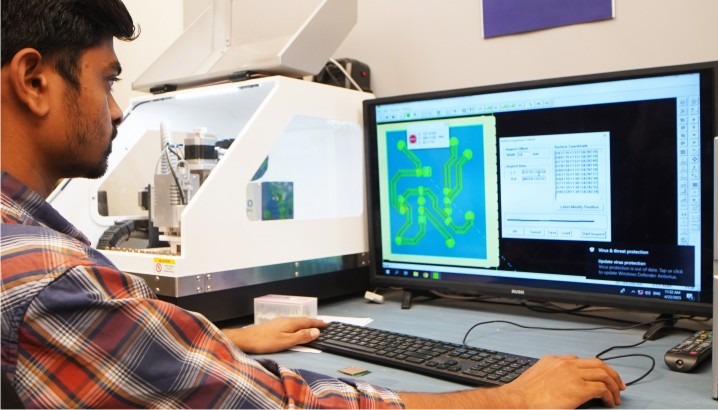
How PCB Machines and 3D Printers transform learning
To address these challenges, educational institutions must incorporate advanced prototyping tools into their labs:
- PCB Machines: These machines enable the fabrication of printed circuit boards directly from digital designs, allowing for rapid prototyping and testing.
- 3D Printers: Essential for creating enclosures and other components, 3D printers facilitate the physical realization of designs, supporting the prototyping process.
By integrating these tools, labs can provide students with a comprehensive environment that supports their entire project prototyping lifecycle, from design to final product.
Delivering end-to-end design thinking solutions
This is where Scientech Technologies comes in, offering a complete suite of solutions that enable institutions to build labs aligned with modern industry practices:
- TINA Design Suite: A powerful tool for circuit simulation and PCB design.
- PCB Prototyping Machines: Including the EP 42 Auto and Nvis 72A, these machines enable the fabrication of PCBs directly from digital designs.
- 3D Printers: Facilitate the creation of physical components and enclosures.
By providing these tools, we empower educational institutions to create labs that mirror industry standards, fostering an environment conducive to innovation and hands-on learning.
Design thinking as the path to innovation
Incorporating PCB machines and 3D printers into electronics labs is not just about upgrading equipment; it’s about transforming how students learn and innovate. With a design-thinking mindset and access to advanced tools, they can move confidently from breadboard experiments to fully functional, validated products. Students become creators, innovators, and problem solvers shaping the future of electronics.
For more information and to explore Scientech’s lab solutions, visit Scientech Technologies website.